


The energy supply of today is based on the use of fossil fuels despite their large environmental impact and the stocks of fossil fuels are diminishing. There is a critical need for developing the renewable energy technologies and the global market of solar cells is growing at approximately 50% per year. Increased cell efficiency and reduced manufacturing expenses are still, nevertheless, utmost critical in making photovoltaics more competitive. Photovoltaic devices of today suffer from very high material cost and low energy conversion efficiencies. Advanced multi-junction solar cells exist and are indeed much more efficient but far too expensive.
The current invention aims at more cost-efficient photovoltaics through a technology, which allows reduced material costs of high-efficiency devices. The invention is based on semiconducting nanowires and piezoelectricity. Nanowires are an emerging technology which offers a large tunability in terms of solar cell materials and device characteristics. Piezoelectricity has, however, never before been applied for photovoltaic applications. The invention could be utilized for stand-alone and grid-connected solar cell applications. Other closely related applications of the invention include light detectors and light emitting diodes.
Figure 1 depicts a piezoelectric nanowire-based solar cell. The array of vertical core/shell nanowires replaces the commonly employed pn-diode of a planar solar cell. The built-in field of a typical pn-diode solar cell is hence replaced by a piezoelectric field, generated by the nanowires. Future developments of the invention are expected to make use of soft polymer-based substrates which would enable elastic and flexible devices.
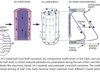
Figure 2 shows the built-in electric field in a single core/shell nanowire, in terms of the potential energy of electrons (charge carriers). The core is made of GaAs and is 100nm thick. The shell is made of GaP and is 30nm thick. The length of the nanowire is 800nm.
Figure 3 shows the operation principle of the invention. GaAs/GaP core/shell nanowires can be created using dedicated vapor phase epitaxy (VPE) despite the different lattice constants of GaAs and GaP crystals. It follows, however, that both the GaAs core and the GaP shell acquire a strain in order to enable the creation of this structure. This strain induces a piezoelectric polarization along the nanowires as a result of the material and crystal properties. This, in turn, gives rise to a built-in field in the nanowires and pn-diode-like device characteristics without a doping of the materials.
Semiconducting nanowires show great promise for high-efficiency photovoltaics but have been hindered by technical difficulties in creating pn-diodes. The fabrication of nanowires and arrays of nanowires is based on – in laboratory environments – established VPE growth. The technique is based on a catalyst assisted self-organization of atoms precipitating from a vapor. The technique is suited for batch semiconductor processing. The material costs of the invention will be reduced considerably by using a silicon (or even a polymer) substrate, in comparison with any other high-efficiency solar cell.
Voting
-
ABOUT THE ENTRANT
- Name:Fredrik Boxberg
- Type of entry:individual
- Software used for this entry:Comsol multiphysics
- Patent status:pending