


The emergence of 24bit recordings has further increased the accuracy of audio material, lowering the THD+N (total harmonic distortion plus noise) at more than -120dB below the audio signal. For transparent sound reproduction, designers are challenged to reduce the THD+N of existing power amplifiers 10 to 50 times to meet the new THD+N milestone.
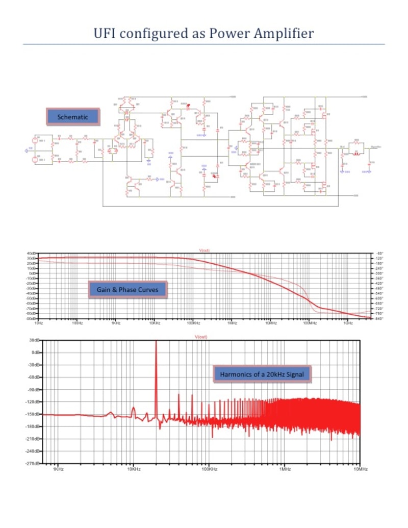
We illustrate a class AB power amplifier (UFI), which according to SPICE simulations may reach a THD+N of -130dB (0.00005% THD+N) at 20kHz into a 4ohm load when configured with a gain of 20. Measurements on a prototype show that the performance depends on the circuit board’s layout and choice of electronic components.
Here are some key design aspects of UFI:
1) Simple, compact and cost effective design with overload protection.
2) Symmetrical circuitry and identical component values at both inverting and non-inverting inputs in either balanced or single ended mode.
3) The symmetrical circuitry configures both inputs with high pass capacitors (C1, C2) of much lower value compared to regular designs.
4) Employs CFP (complementary feedback pair) configurations across every amplification stage.
5) Scalable power to more than 1000W.
Here is why the use of CFP configurations in UFI allows for very low THD+N:
1) A CFP configuration provides better linearity and lower distortion than other configurations (Darlington or cascade).
2) The input stage CFP configurations (Q1-Q2, Q3-Q4) provide in addition increased gain to reduce the noise contribution of the VAS (Voltage Amplification Stage) and output stage. While Q1 and Q3 function at optimal current for lowest noise, Q2 and Q4 provide sufficient current for charging/discharging capacitor C6 and providing a high slew rate (60V/?s).
3) Simulations show that configuring the VAS with a cascode configuration instead of a CFP configuration will increase the open loop gain for a same THD value. The increase in open loop gain would make the circuitry more sensitive to parasitic influences. So we preferred a CFP configuration (Q9-Q10) in the VAS.
4) The triple CFP configurations (Q14-Q16, Q17-Q19) in the output stage provides extra gain and high output impedance for the VAS, which means less overload, more linearity and lower distortion.
Since the distortion components are at or below the noise level, reducing the amplifier’s noise, especially the thermal noise produced by the resistors, will lower the THD+N. Emitter resistors R10 and R11 can be absent.
Furthermore, a low THD+N can be achieved by inserting a buffer in front of the UFI power amplifier, and distributing the closed loop gain among them. In this case, the UFI power amplifier can have lower input impedance and gain, employ resistors with lower value at both inputs and feedback loop, and therefore reduce the thermal noise.
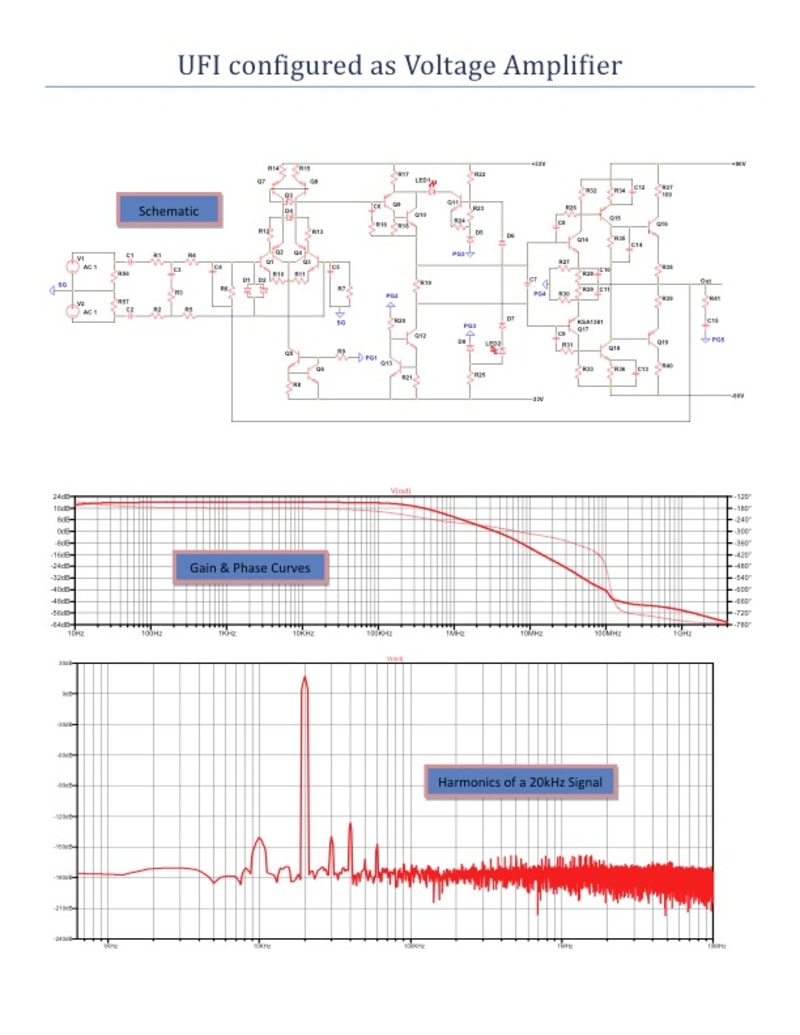
The second figure shows a similar schematic that can be used as a voltage amplifier. When configured with a gain of 5 the simulation shows that the voltage amplifier and UFI power amplifier exhibit a THD+N of 0.000010% and 0.000017% respectively.
Like this entry?
-
About the Entrant
- Name:Ioan Salomie
- Type of entry:individual
- Software used for this entry:LTSpice, Adobe, MS Office
- Patent status:pending