


NASA’s Langley Research Center has developed a novel method of depositing metal and metal oxide nanoparticles onto various substrates (see ACS Nano, 3(4), 871–884 [2009]). It is rapid, scalable, and green since it does not require reducing agents or solvents. The process involves first mixing and then heating a metal salt (usually an acetate) with the desired substrate. Heating can be done by conventional thermal or microwave ovens. Conventional thermal processing takes several hours and requires an inert atmosphere, usually nitrogen. With microwave heating, the process is complete in a matter of seconds. The metal or metal oxide nanoparticles have potential use in electromagnetic applications. The nanoparticles have been evaluated for electromagnetic properties at high frequencies for potential antenna applications (S. Ghose, et al. SAMPE Electronic Conference Proceedings, [2009]).
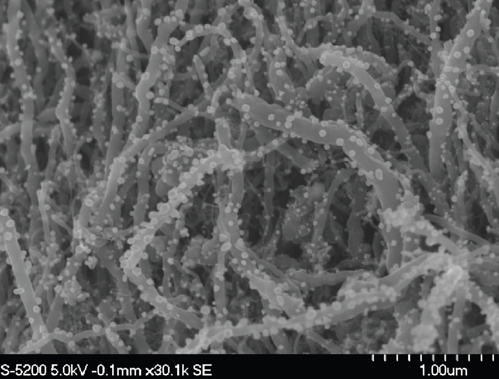
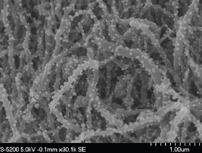
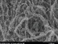
NASA’s technology involves the development of tailorable dielectric materials by the deposition of metal nanoparticles on carbon nanotubes using a solvent-free
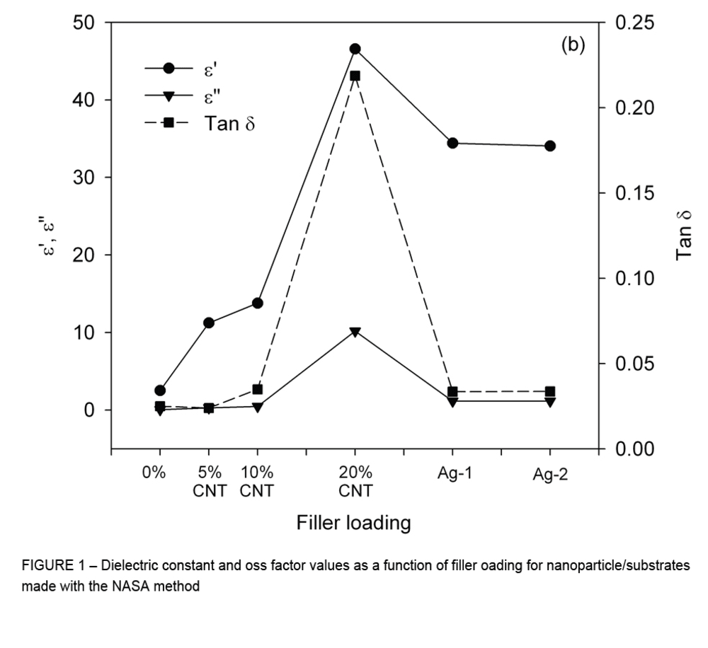
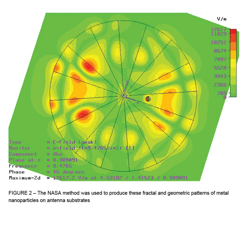
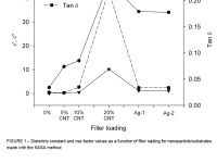
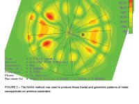
method. The novel materials consist of aligned nanotubes decorated with nanometer dimension metal particles distributed in a polymer matrix. The tailorable complex permittivity parameters allow for an increased dielectric constant (e’) with a decreased loss factor (e”) (Figure 1). In addition, varying the amount of metal particles attached to the substrate surface can control the disconnection between the dielectric constant and the loss factor. The decoupling and independent control of these fundamental electrical material parameters afford a class of materials useful in a variety of applications in electronics, electromagnetics, and microwave engineering, with potential future applications in the optical frequency regime. Specific applications include the fabrication of fractal and geometric patterns (Figure 2) in antenna substrates, thereby improving antenna performance. The technology is described in patent application 20090022977, US Patent 7,704,553, and in NASA disclosures LAR-17638-1 and LAR-17427-1.
Tailorability of the materials allows for innovation of new products:
-Low-mass, ultra-thin microstrip antennas with enhanced performance
-Fractal antennas for cell phones
-Radio frequency identification antennas
-Very thin, low-profile substrates for high frequency electronics
-Higher capacity low-volume capacitors
-High-Q dielectric resonators useful in high frequency oscillators and filters
-New anode/cathode materials for efficient low-resistance, low-loss battery components
-Components of various multifunctional material systems, particularly as materials for High-K gate dielectrics in complementary metal-oxide-semiconductor (CMOS)
technology
-
Awards
-
 2015 Top 100 Entries
Like this entry?
-
About the Entrant
- Name:Kathy Dezern
- Type of entry:individual
- Patent status:patented