What CopperPak does
Complex microprocessor are important, but simple discrete diodes are similarly indispensable. Conventional wisdom is squeezing everything onto the same wafer, yet, just not all components can go on the same wafer. A power-supply diode should not go on the same semiconductor of a microprocessor. An electrostatic discharge (ESD) protection component is better installed close to but off the microprocessor it protects. Together, digital processors and discrete components deliver the designed system functionality. Failure of CPU means a broken computer, but a bad power diode still brings down the system.
Core semiconductor of all devices requires proper packaging, processors and diodes alike. Core of a diode coming off the production wafer must be sealed within a protective packaging, and it also needs to dissipate operational heat. CopperPak is an efficient technology for electronic device packaging. The technology is based on a simple philosophy of taking copper, optimally the best material in terms of both electrical and thermal conduction, as the core material for packaging.
The principle is known, but none comes close to CopperPak in terms of performance and reliability. When compared with conventional devices of the same size specification, a CopperPak device performs significantly better. When compared at the same performance level, a CopperPak device is at least one size smaller. Thus, space is saved. Or, performance is improved. In some cases, both are achieved.
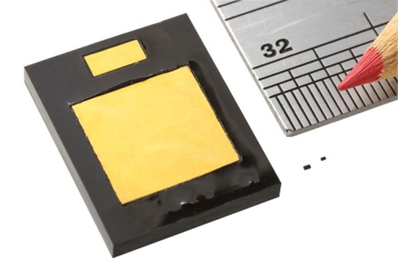
Built under CopperPak, an ESD diode withstands substantially higher current, and a power diode handles larger current. A few CopperPak 0201 ESD component types have surpassed protection voltage rating of conventional 0402 devices up to +/-15,000 volts (IEC 61000-4-2). CopperPak is not only for tiny devices down to JEDEC 01005 and smaller, it’s also suitable for big devices. A JEDEC TO-268-sized power diode to the military standard has been made. CopperPak manages to deliver much improved power rating while its physical size is reduced. This means a CopperPak 0201 ESD component can be responsible for circuit protection task taken up by a larger 0402.
How CopperPak works
CopperPak is based on two guidelines. First, copper is effectively the single material used as the “vehicle” for CopperPak. Sheet copper is not only used as the production-phase substrate but also made into the final electrical conductor for CopperPak components. Single copper use means there’s no need to compromise among a set of complex and inevitably mutual-contradicting processing conditions if more than one material are involved for the packaging, as in the conventional use of PCB. CopperPak improves batch-production efficiency by an order of magnitude of up to 2: Tens of thousands of product components per array-batch compared to hundreds delivered by conventional technology. Single use of copper results in simplified processing methodology, which reduces cost.
Secondly, CopperPak recruits the use of existing matured copper-processing technologies in parallel industries. With adaptation, low-cost rudimentary PCB manufacturing techniques like etching and electroplating are adopted. Benefits are obvious. Matured techniques mean less unexpected problems. And, as PCB is so ubiquitous, the cost is very low.
-
Awards
-
 2016 Top 100 Entries
Like this entry?
-
About the Entrant
- Name:Norman Chang
- Type of entry:individual
- Patent status:patented

