

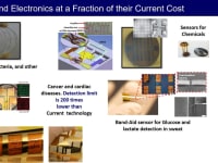

Nano OPS, Inc. is a spinout from Northeastern University with a mission to “democratize” nanomanufacturing, making it more broadly accessible to industry and entrepreneurs. Current semiconductor tools cost between $5 million to $150 million each and require manufacturing facilities costing billions of dollars to construct and more than a billion dollars/year to operate.
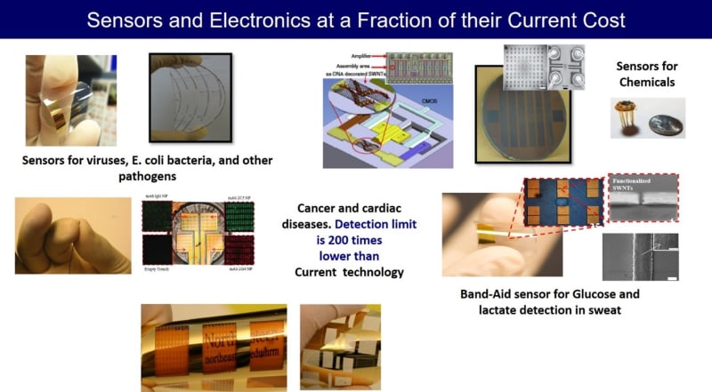
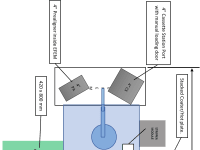
Our directed assembly-based nanoscale manufacturing platform is revolutionary new nano and microscale electronics manufacturing system. It utilizes basic physics and physical chemistry to direct the assembly of nanoscale particles or other nanomaterials in suspensions in a room-temperature, atmospheric pressure onto a substrate precisely to print electronic devices. The technology is a radical departure from conventional semiconductor manufacturing techniques which require thousands of process steps comprising of high energy deposition processes followed by aggressive chemistry for etching. Using the Nanoscale Manufacturing Platform, multiple material layers of the same or different material can be printed on previously printed structures by repeating the directed assembly process. The technology enables the creation of 0D, 1D, 2D, and 3D structures with the desired combination of materials down to nano-scale structures (demonstrated to 20 nm structures). All at a fraction of the cost of conventional fabrication equipment. The Nano OPS manufacturing platform has been proven for its effectiveness at wafer-scale manufacturing and currently producing devices on the 4" (100mm) wafers.
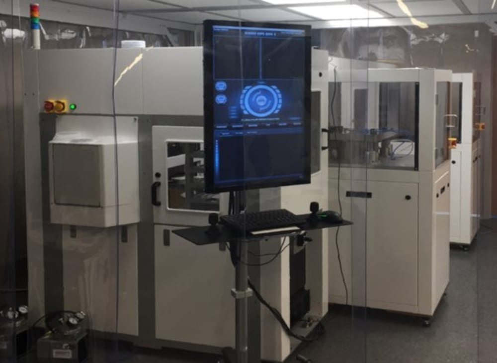
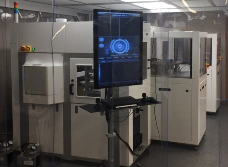
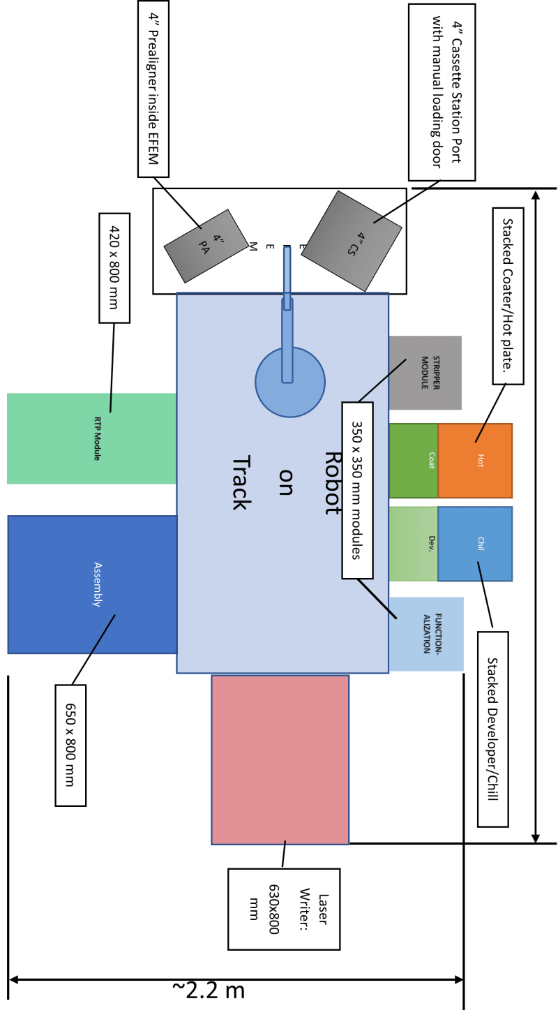
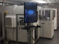
Designed for research and development, suitable for customers in industry, government, and academia. The Fab-In-A-Tool is fully automated equipment that takes a CAD input and prints the pattern directly on the substrates. The equipment has an integrated that includes a robot for handling substrates, lithography module with coater, developer, stripper, and laser writer for patterning. This equipment can print feature size is down to 800 nm, deliver multi-layer alignment down to 2µ between layers. The tool is capable of printing a single layer in under 40 minutes and occupies approximately 6 square meters of space. The technology has been used to print conductors, semiconductors, dielectrics, and CNTs. The tool starts at a price of $1.5 million each and can be housed in a garage to begin producing integrated circuits. The key benefits are:
- Eliminating high energy deposition processes such as CVD, PVD, ALD, Electroplating, and etching.
- Using a very small amount of material – up to 1000x material saving,
- Reduction of 100s of steps at smaller feature size.
- Freedom to choose the optimal material (organic or inorganic semiconducting, conducting or insulating material on flexible or rigid substrates) best suited for a specific design.
- Build heterogeneously integrated functional systems (system on a chip.)
- Fraction of capital cost (up to 10 x less) and operational cost (up to 1000 x less)
-
Awards
-
 2021 Top 100 Entries
Like this entry?
-
About the Entrant
- Name:Sudhir Jain
- Type of entry:teamTeam members:Ahmed A. Busnaina, CTO, Nano OPS, Inc.
Sudhir Jain, CEO, Nano OPS, Inc. - Patent status:patented