


Material scientists have made tremendous efforts for the miniaturization of computer processors both in the industries and the academic sectors. Here, we have approached a physical limit of silicon technology, where Moore’s law cannot be challenged. In the era of colossal technological advances, it has become imperative for materials to have extraordinary properties and bring intriguing technologies. The atomic layer of stretchable 2D materials of conductors (graphene) and semi-conductors (molybdenum disulfide, MoS2) are potential candidates to replace silicon (Si) or synergise with it for the development of the tiniest transistors, ultimately a chip of an ultra-fast computer processing.
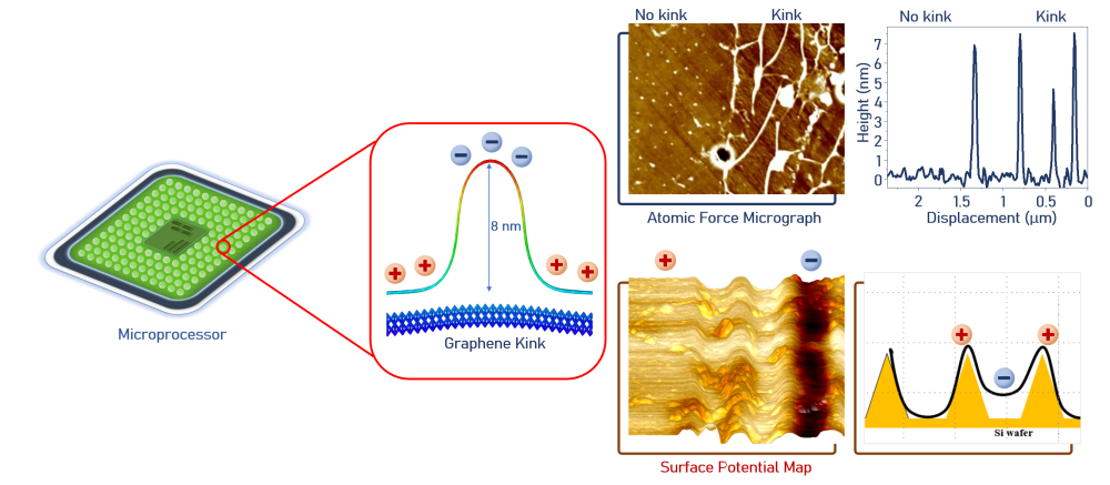
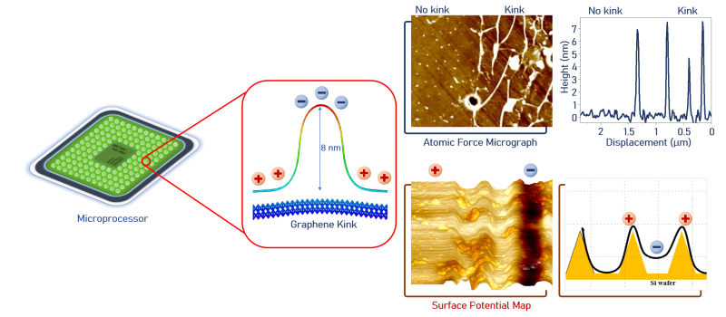
The solution lies in the nanotechnology of stretchable materials. A blend of mechanics and electronics called “straintronics” has been known in recent years, where desired electronic properties of the materials can be achieved by straining (compression/tension). We have used this technology to develop a kink (or gap from the substrate) in the 2D materials with a height up to 8 nm and width around 2.5 nm. The kink/gap acts as a localized center of different electronic charges from their surroundings and lead to p-n-p or n-p-n transistors (see figure: surface potential map) [1]. Thus, a series of kinks of 2D materials accommodate millions of transistors in a millimeter square area. We developed two different hybrid surfaces as a proof of concept in our laboratory for the fabrication of the smallest transistors. Alternatively, these surfaces also act as an ultra-sophisticated electromechanical sensors.
Proof of concept 1 (manipulating structural defects): We have developed the experimental set-up to fabricate the series of graphene wrinkles on our hybrids surface of Si wafer (Si/silica/MoS2/graphene) by mimicking a natural phenomenon of the ageing of the skin in living beings. At old age, the outer layer of skin (epidermis) gets stiffer than the inner layer (dermis), and this difference in mechanical properties leads to the generation of wrinkles as the outer layer tends to accommodate the extra surface area during contraction of inner layer. Similarly, graphene (nearly three times stronger than MoS2) over MoS2 compresses the subsurface and gets wrinkled itself (see experimental figure: Atomic force microscopy). There is an additional factor of inter-layer slipping that favours the wrinkle formation (see figure: simulation). Thus, we successfully generated wrinkles at the desired locations using vertical hybrid heterostructure.
Proof of concept 2 (laser induced texturing): Graphene-Si is a p-type doped system, and thus a textured induced gap can prohibit such doping at localized area leading to p-n-p transistor (see, surface potential map). One must be aware that graphene sagging at the trough region should not touch the silicon surface to avoid the p-doping. The suspension of graphene can be achieved by milling smaller width of the groove.
Our findings on the hybrid surfaces is a key step forward towards game-changing technology for introducing more chips inside a device, fast computing and sensing.
Reference:
1) ACS Nano 2021, 15, 2, 2520–2531.
https://doi.org/10.1021/acsnano.0c06701, https://acs.altmetric.com/details/98635546/news
-
Awards
-
 2021 Electronics/Sensors/IoT Honorable Mention
 -
 2021 Top 100 Entries
Like this entry?
-
About the Entrant
- Name:Manoj Tripathi
- Type of entry:teamTeam members:Dr. Manoj Tripathi: Department of Physics and Astronomy, University of Sussex, Brighton BN1 9RH, U.K.
Frank Lee: Department of Physics and Astronomy, University of Sussex, Brighton BN1 9RH, U.K.
James G. McHugh: Department of Chemistry, Loughborough University, Loughborough LE11 3TU, United Kingdom - Patent status:none