
Overview
We are augmenting an existing opposing super magnet array for advanced shock mitigation footwear called DAMPS Technology D Drives to provide an alternate renewable energy source powered by every step you take. The D Drive was developed over ten years with USSOCOM Special Operation Forces (SOF) and recorded/reduces heel strike nearly 70% each and every step.
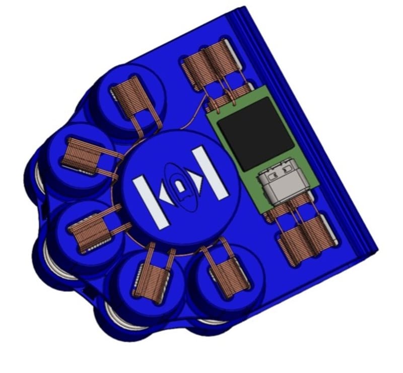
The D Drive 5.0, as measured, produces 2-3 joules watts of DC current in linear walking motion. Our plan is to further design and add a) advanced copper coil(s) windings and b) add a select IC Chip from Texas Instruments (TI) to modulate, amplify and store the electron load current induced by the overlapping magnetic polarity fields produced within the D Drive.
The D Drive utilizes two opposing 35 MGO neodymium rare earth magnets and as measured with a Newton meter in a prototype jig, produces 2-3 joules watts of DC current in linear biomechanic walking motion.
TI has suggested an IC Chip (BQ25505) for low ultra low power IC management with boost charger and autonomous power multiplexor, based on our magnetic array in the D Drive. The TI IC Chip will be developed and with a EVM prototype board provided by TI and other third party specialists, until we have maximized modulation DC current flow and charging output. B&B worked with TI support over a year before the pandemic.
Intellectual Merit
Beyond the unique proprietary and non obvious shock mitigation delivered by the D Drive, the addition of our proposed DC motor coil windings with an IC Chip for continued DC power flow and harvesting for external battery and/or modular plug in charging is a game changer. With today’s battery and electronic dependent culture and device charging demand, this alternate power charging source is a needed break through to fully explore all possibilities.
The BQ25570 EVM
To determine the actual current, we are producing energy, we can use a current shunt monitor but it will bleed off some of the current through the sensing resistor. If the current is small, we might be able to use something like the INA216 as it has the lowest current usage. We could use this to actually test the flow, but we probably would not use it in the application as it would take some energy to operate and the level of energy as described is low.
The EVM is a prototype circuit that we could use to test our application. Once we receive the EVM we can board test your application to see if it works. We can change the components on the board if need be to mimic the application that we want to do. That is why they are advantages. We do not have to design a board to test your applications will work. The EVM board can do this and it will save time.
The EVM was designed to test our application. Texas Instruments produces the board and we
can use it to verify that your application will work.
Like this entry?
-
About the Entrant
- Name:Jeff Brown
- Type of entry:individual
- Software used for this entry:Solid Works