


Two-dimensional detector arrays of thermal infrared imagers are expensive, especially at medium and high resolutions. A 10,000 pixel imager costs about $1,600. An 80,000 pixel device costs about $5,500, and an imager with near 3x105 pixels costs about $20,000. Now assume that, instead of the bolometric arrays of present thermal imagers we place a thin, strongly fluorescent film in thermal contact with the infrared-absorbing layer and illuminated from the sides to excite the fluorescence of the film in such a manner that the infrared image focused on it will be converted into a corresponding visible image at the film, ready to be focused on and processed by an inexpensive digital camera. High resolution would no longer be expensive: a 16 Megapixel camera costs about $100.
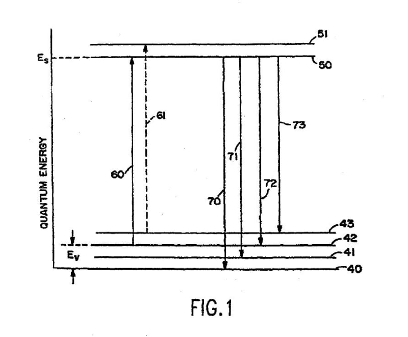
In order to function as described above the fluorescent material of said film must emit, at any resolvable point, a strongly temperature-dependent fluorescence intensity when illuminated with light of wavelength within the long wavelength ‘tail’ of a strong electronic absorption band. Virtually all solid fluorescent materials show this property. It has been known for nearly a century that the absorption of light within such long wavelength ‘tail’ is strongly temperature-dependent, but this knowledge was not applied to make a useful device. The physical basis of this behavior is shown with the (simplified) illustration of FIG 1, which is a schematic molecular energy diagram applicable to most compounds, taken from submitter’s US patent 7,586,106. Using the same labels as the patent figure, energy level 40 is the ground electronic level, and levels 41-43 are its vibrational sub-levels. In a statistically large ensemble, the number N42 of molecules occupying level 42, with an energy Ev higher than level 40 follows the Boltzmann distribution
N42 ≈ N40.exp(-Ev/kT), where k is the Boltzmann constant.
The absorption coefficient αT, being proportional to N42/N40, can be expressed as
αT = K.exp(-Ev/kT), where K is an instrumental constant.
The generated fluorescence intensity If is proportional to αT and the temperature coefficient of the fluorescence intensity generated at each pixel is (1/If0)(dI fT/dT) = Ev/kT2
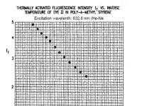
FIG 2 (FIG 3 in the cited patent) confirms the validity of the temperature measurement method. The Figure indicates a temperature coefficient of about 0.02 per kelvin within the range, but substantially higher coefficients are achievable. For a given practical value of (Ev/k) said temperature coefficient greatly increases with decreasing temperature.
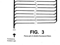
FIG 3 shows an alternate embodiment of the thin fluorescent converter as an etched planar grid of ultra-thin fibers. In thermal contact with the infrared absorber.The fluorescent converter need not cover the whole area of the infrared absorbing pixel. The thermal mass of the converter, then, could be much smaller than that of the infrared absorber. The relatively long optical path length of the interrogating light permits moderate concentrations of the fluorescent material.
-
Awards
-
 2013 Aerospace & Defense Honorable Mention
 -
 2013 Top 100 Entries
Like this entry?
-
About the Entrant
- Name:Marcos Kleinerman
- Type of entry:individual
- Patent status:patented