


Electroplate and Lift (E&L) Lithography is high-throughput, high-volume manufacturing of patterned nanowires and microwires. Unlike traditional nanomanufacturing, requiring a costly clean room full of equipment, our technology is a simple electroplating bath, power supply, and one of our reusable Ultrananocrystalline Diamond Template (UDT) electrodes, designed to produce any pattern desired. This new technique makes nanomanufacturing of complex nanowire circuits so easy, we created the NanoFab Lab … in a Box!™ This shoebox-sized kit allows high school students to manufacture hi-tech patterned nanowires in the classroom. This introduces students to nanotechnology and practical nanomanufacturing.
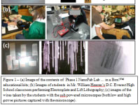
NanoFab Lab … In a Box!™ Educational Kit is a product that brings the technology to high school and post-secondary students. It provides a connection between their curriculum and the emerging field of nanotechnology and nanomanufacturing. The kit contains everything with the exception of water and inexpensive chemicals for allowing students to grow nanowires. The UDT electrodes get connected to a hand-held, battery-powered, web-enabled instrument called a potentiostat that allows precise control over the electrochemistry and records data for analysis. The wires produced may be imaged using a 700X USB powered microscope allowing students to measure wire quality and size. Both the potentiostat and the microscope connect to an included 10” Android tablet for uploading their data, images and videos through a secure web portal. The website documents their progress and gives feedback for how to improve the quality of their wires. The NanoFab Lab … in a Box!™ educational kit produced by a non-profit educational organization represents a first of its kind and first to market nanotechnology product for an audience that needs hands-on educational tools.
A recent report by the US Government Accountability Office states “Nanomanufacturing is a future megatrend that will potentially match or surpass the digital revolution’s effect on society and the economy.” Broad statements like that illustrate our nation’s hope for nanotechnology to be a potential solution for some of society’s most vexing technological challenges. However, the development of nanotechnology resources for education, especially at the K-12 level, is lacking. The NanoFab Lab … in a Box!™ provides students the tools to discover novel nanowire compositions and innovate new applications for nanotechnology. This unique program stimulates the interest of bright students and retains their talent in STEM fields.
In addition to the education aspect of this technology, the same concept will be very useful for nanomanufacturing on mass-scale. Combining different patterns with different transfer techniques, from something similar to a printing press to something analogous to a continuous conveyor-belt, allows the design of an unlimited number of patterns, devices, and components that can be used in everything from functionalized biomedical particles, to massively-redundant structural monitoring sensors, to large-scale printed electronics on any shape surface, or printed nanowires for solar cells, etc. all at volumes and costs previously unthinkable because E&L breaks the nanomanufacturing clean room paradigm. E&L provides a practical, cost-effective alternative nanomanufacturing technology.
Video
-
Awards
-
 2014 Consumer Products Category Winner
 -
 2014 Top 100 Entries
Like this entry?
-
About the Entrant
- Name:Dr. Michael Zach
- Type of entry:teamTeam members:Dr. Michael Zach, Dr. Anirudha Sumant, Jonathan Moritz
- Software used for this entry:Microsoft Office, 3ds Max
- Patent status:patented