

The GPX2 Time to Digital Converter (TDC) is designed for applications where high single shot resolution to 10 picoseconds, best pulse pair resolution of 4 nano seconds and high measurement rate are required. The GPX2 is ideal for high end LIDAR, spectroscopy, medical and a variety of military applications requiring high performance and reliability while still having low power consumption that is compatible with battery powered devices. These devices can also be used to measure high speed rising and falling edges as well as pulse widths, making them ideal for automated test equipment. The GPX2 is also very suited to high energy physics time of flight applications including single photon counting.
The GPX2 is the latest in a long line of commercially available Time to Digital Converters from our partner ACAM, who pioneered the commercially available TDC. ACAM has almost 2 decades of experience in perfecting the TDC technology and the GPX2 continues to pioneer new territory. Their compensation methods for temperature and voltage variations guarantee high stability and repeatability.
The timing principle is to use an array of buffer delays. Intelligent circuit structures, redundant circuitry and special methods of on-chip layout to permit the GPX2 to determine the exact number of gates that a signal passes through, resulting in the time being measured accurately. The TDC is started from a common Start signal and up to 4 Stop channels can be used to capture timing events. The GPX2 inputs are configurable to be sensitive to rising and / or falling edges. Each channel has a 16 stage FIFO to capture high speed events.
This 4 channel TDC has LVDS inputs and outputs making it ideal for pairing with FPGAs or high end microcontrollers. The format of the output data is a start retrigger number that can be configured from 0 to 24 bits and a timestamp that is configurable in either 16 or 24 bits in length allowing very large time intervals to be accurately measured. Optionally, for short events, you can eliminate the start retrigger number and use just the 16 bit timestamp to improve data throughput.
The device registers are configured over a SPI bus, keeping the LVDS lanes clear for high throughput data. However, for testing and low data speed applications, data can also be read out over the SPI bus.
The GPX2 is based on standard CMOS processes and has 3.3 volt I/O and a core voltage of 1.8 volts that is supplied by the internal 1.8 volt regulator. The typical total current is less than 80mA and the operational temperature range is -40 to +125 degrees centigrade.
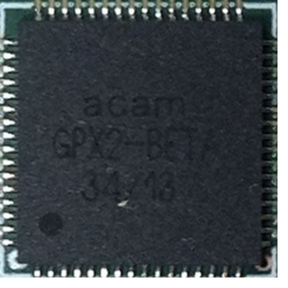
The GPX2 is packaged in a small QFN package for easy board assembly.
-
Awards
-
 2014 Top 100 Entries
Like this entry?
-
About the Entrant
- Name:John Monteith
- Type of entry:individual
- Patent status:pending