


Currently, manufactured parts are inspected with a device known as a Coordinate Measuring Machine (CMM). These machines use an electronic probe tipped with a ruby or ceramic ball. The probe presents the ball in motion (via mechanical elements driven by servo motors) at a precise vector to the surface of the part and records the timing, intensity and deflection angle of that ball to determine the exact point at which the probe makes contact with the part under inspection. The probing points are recorded in specialized software and the measurements are calculated by interpreting the points and extrapolating what the surface of the part may be like from that data.
A highly skilled programmer is required to create the probing routines needed to move the probe around the part without collisions and rotate the probing head to different approach angles as needed to present the ruby ball at the appropriate vector angle normal to the surface. He or she must also determine how many points to probe and where to best place them for the most accurate measurement. Even though a part small enough to fit in one’s hand may have a hundred probed points on it, only a minute fraction of the total surface area will be represented. For example, a hole is commonly defined with only three or four points regardless of the size of the hole. This leaves almost the entire circumference unprobed. Any “out of tolerance” conditions in unprobed locations are missed entirely.
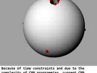
I propose a CMM that will utilize nanoprobes consisting of miniature RFID chips (such as Hitachi’s new RFID “powder”) embedded in the center of ruby or ceramic spheres of, for example, .5mm diameter. These spheres could be contained in a bin (perhaps a half-spherical “bowl” shape) which would have receivers embedded around the inside of it to triangulate the true position of each of the RFID chips. A part would then be submerged into the bin of nanoprobes and lightly shaken or vibrated in order to allow the nanoprobes to equally distribute and come to rest against the entire surface of the part. This innovation would make inspection of manufactured parts easier, faster, and more precise.
Additionally, nanoprobes could reach difficult to access surfaces which are currently (virtually) impossible to measure without resorting to destructive measuring techniques. If one imagines submerging a whiffle ball into the inspection bin, the nanoprobes would pour through the holes to fill the ball and report their position next to the inside surface of the ball as well as the outside. Since the current technology will allow each of the Hitachi chips to have a 128 bit ID number, probing data can potentially be collected from as many as 10^38 unique sensors.
Once the price of the technology equalizes, this could also have applications wherever a surface needs to be mapped or measured. (Pipelines, space exploration, medical imaging etc.)
References:
1. RFID "Powder" http://www.hitachi.com/New/cnews/060206.html
2. CMM measurement strategies: David Flack: http://publications.npl.co.uk/dbtw-wpd/exec/dbtwpub.dll?&QB0=AND&QF0=ID&QI0=2771&TN=NPLPUBS&RF=WFullRecordDetails&DL=0&RL=0&NP=4&AC=QBE_QUERY
Like this entry?
-
About the Entrant
- Name:David Hawkins
- Type of entry:individual
- Software used for this entry:Rhinoceros 3D modeling software
- Patent status:none