Problem
There is a need for nanoscale pores and slits for nanotechnology medical and research applications that cannot be produced using even state of the art lithography and etch technology. More specifically, pores and slits with dimensions down to less than 10 nanometers cannot be made reproducibly with full tunable control. Consequently, the tools available for applications such as DNA analysis, blood cell or other particle counting, nanofluidics, and numerous others are costly and inefficient at best.
Approach
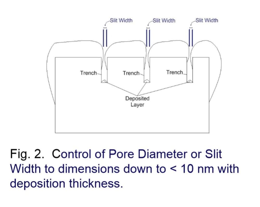
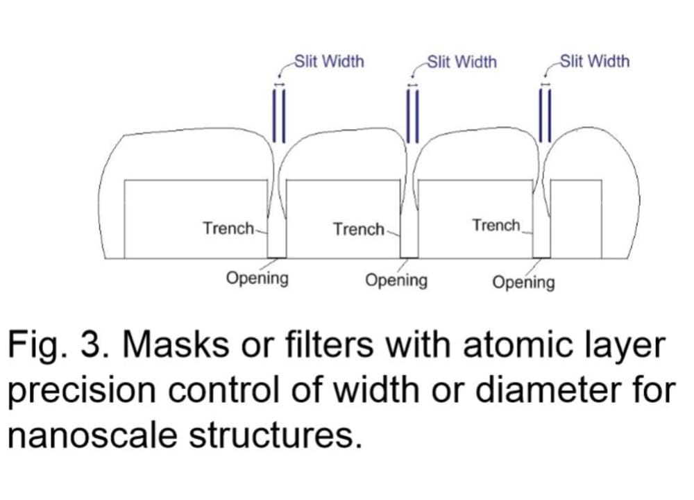
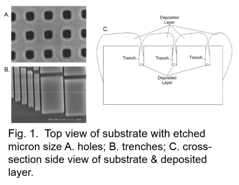
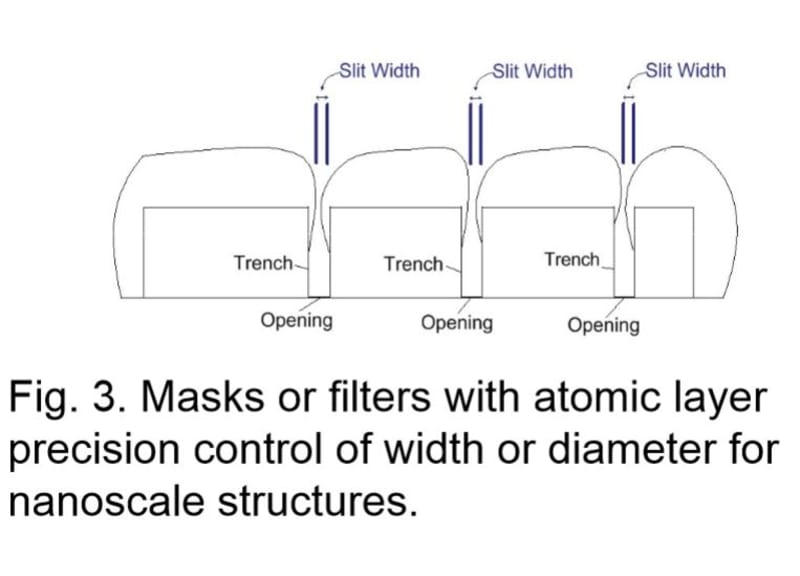
This new idea uses technologies that may be > 20 years old to produce trenches and/or holes in substrates. Fig. 1 shows examples of holes Fig. 1A and trenches Fig. 1B formed on a substrate using processes from the 1990’s. The holes in Fig. 1A and the trenches in Fig. 1B are about 1 micron in size. The new idea uses structures like those in Fig. 1A & 1B (or even larger structures) and current technology thin film deposition processes. A layer is deposited over the substrate as shown in cross-section in Fig. 1C and Fig. 2 to form pores and/or slits from the holes and trenches. The pores and slits have nanoscale dimensions. Fig. 3 shows a cross-section side view with the bottom portion of the substrate removed to form open bottom pores and slits for masks or filters.
The deposition processes may be nonconformal and/or conformal such as physical vapor deposition and some types of chemical vapor deposition. Also, conformal chemical vapor deposition processes such as atomic layer deposition can be used for fine tuning. The processes may also use etch processes to adjust the deposited layer. Amorphous materials may be preferred when forming smaller dimension structures.
Overall, the processes achieve atomic layer precision in controlling widths and diameters for nanoscale structures.
Benefits
This idea will allow the use of less expensive equipment to produce nanoscale and sub nanoscale pores and slits. The pores and slits can be made using a variety of materials and also fabricated in essentially any desired patterns. Filters and shadow masks with nanoscale and sub nanoscale selectivity can be made easily and economically using well established semiconductor processing methods and facilities.
This idea will provide complete control of the dimensions of pores and slits to possibly less than 10 nanometers. This idea will be a useful scientific tool for the research and business community particularly in medicine, research, filtration, analysis and many other fields. The methods and products derived from the present idea will serve a large market.
Competition
Today's advanced lithography and etching techniques are unable to produce structures like those of the present idea. Also, they probably will never be as cost-effective as this idea. Failure to pursue idea could delay or prevent some advancements in research and analytical techniques and in medical technology.
Like this entry?
-
About the Entrant
- Name:Larry Williams
- Type of entry:individual
- Software used for this entry:TurboCad
- Patent status:pending


