


NASA’s Jet Propulsion Laboratory has developed an imaging device called an active pixel sensor that is inexpensive and easy to fabricate. The active pixel sensor is designed to perform at least as well as conventional charge coupled device (CCD) imagers without all the drawbacks. CCD imagers are susceptible to radiation damage, require good light shielding to avoid smear, and have high power dissipation for large arrays. In addition, the CCD fabrication process is incompatible with complementary metal oxide semiconductor (CMOS) processing, which makes it difficult to integrate on-chip signal processing electronics. JPL’s active pixel sensor, which can be fabricated using an industry-standard CMOS-compatible process and smaller-sized pixels, is an integrated imaging device that is well-suited for a variety of applications, including guidance & navigation and robot vision.
JPL’s active pixel imaging device comprises a focal plane array having a simple
floating gate (SFG) pixel structure and a readout circuit. An SFG sensor array can
be implemented using an industry-standard CMOS-compatible fabrication process,
allowing the readout circuitry to be implemented as inexpensive CMOS circuits.
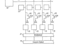
A column-parallel approach—in which an entire row of the array is processed
simultaneously—frees up additional photosensitive cell area and thus improves
resolution. In addition to a transparent refractive microlens layer, which can be
contoured to focus light toward the center of each photogate, an optical shielding
layer can be used to shield the non-photosensitive portion of each pixel cell and thus
minimize noise effects. An intermediate transfer gate and storage potential well can be incorporated to allow for the simultaneous integration of the array. Combined with the sensor’s non-destructive readout capability, these supplemental gates make JPL’s imaging device ideal for capturing faint objects.
A 32 x 27 active pixel sensor with a pixel size of 40 x 40 ?m has been implemented in
a 2-?m double-poly n-well CMOS process. The photogate voltage varied linearly with the amount of accumulated charge and no blooming was observed.
BENEFITS
* Integrated, on-chip signal processing is cheaper and more efficient
* A transparent refractive microlens layer focuses light onto the photosensors
* A column-parallel array structure improves the resolution of each pixel
* Non-destructive readout capability is ideal for low light imaging application
(The first illustration is a plan view of a focal plane array suited for use with a column-parallel approach. Each pixel cell 15 in a column of the array is connected to a common load field effect transistor 65 and sampling circuit 70. The column-parallel array structure is read out by selecting an entire row using standard row and column select circuitry 18, 19 and outputting the read pixel values using a standard multiplexer 21.)
-
Awards
-
 2015 Top 100 Entries
Like this entry?
-
About the Entrant
- Name:Erick Fossum
- Type of entry:teamTeam members:Erick Fossum, Junichi Nakamura, Sabrina Kemeny
- Patent status:patented