


Our ultra-small inverter, designed in 2015, allows converting DC high voltage into residential AC voltage. A prototype was built in Q3 2015. Existing similar converters currently on the market are more than 30 times bigger.
Our tiny design enables new opportunities, especially in the renewable energy field. Indeed, the converter could easily fit in an electric car or any other mobile embedded system to supply any household device from a high voltage battery. Similarly, several converters could be installed in a house’s structure, and benefit from a high voltage battery to supply all the household devices. This battery could supply on different sources: solar panels, wind turbine, water turbine, electric car or power grid. Homes in remote areas or humanitarian service centers could benefit greatly from this type of electrical installation, which may be independent of the electrical distribution network or gasoline. Some credible and powerful companies like Google have shown publicly their interest in reducing the size of the currently available power inverters that have similar specifications to our high density design.
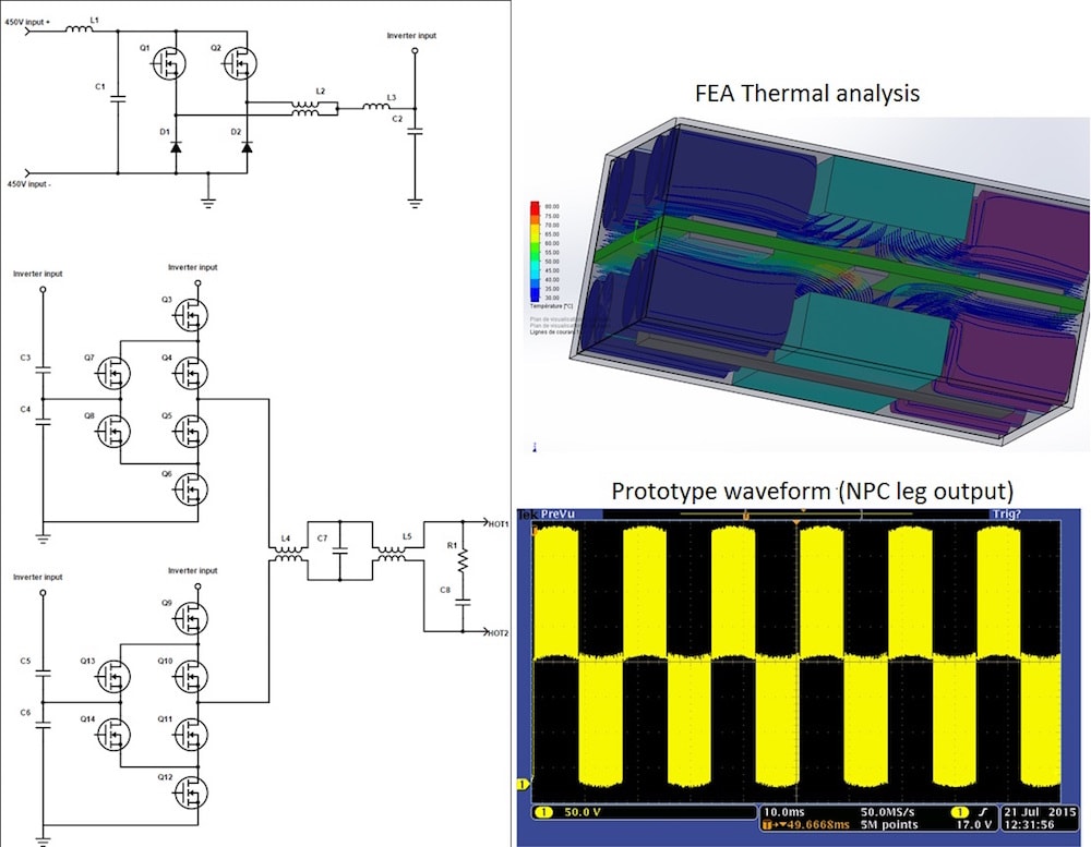
Our converter uses several technical advances and new technologies to achieve its impressive power density. The use of Gallium Nitrite EPC devices in a two NPC legs topology allows high switching frequency, high efficiency and lowers the requirements for the output filter. An innovative control scheme is used on the inverter to limit the simultaneous switching of both legs stressing the output filter. An input dc-dc converter driven by 3 nested software control loops provides low voltage ripple on the input. Silicon carbide diodes and high speed Mosfets allow high efficiency. The high frequency two stages output filter and the magnetics used in the input stage are carefully designed to fit in a specific location while providing a standards-compliant sinewave at the output and a smooth input current ripple. The maximum input voltage ripple is 1.5% and the whole device is designed for electromagnetic compatibility.
These high-tech features were also thought and implemented to optimize the ease of assembly and the mass production costs. Indeed, the device is made of a single printed circuit board, including some power and control circuitry carefully decoupled and interfaced. This unique PCB assembly contains all the electronic components, and the few connectors and fans also needed are assembled on a standard steel enclosure prior to the final assembly of the PCB into the enclosure. The high efficiency and the mechanical design limit the need in thermal management components like thermal pads or thermal grease, which are costly and laborious to manufacture. The PCB is designed so any PCB assembly plant, which is familiar with the current state of the art, can perform the soldering operations required. All the selected components are available off the shelf. In mass production, the cost will be driven by the raw materials, so our design cost would surely benefit from its size. Also, trends in the GaN devices market show significant short term cost reduction, mostly caused by the current increase in production volumes.
-
Awards
-
 2016 Electronics Honorable Mention
 -
 2016 Top 100 Entries
Like this entry?
-
About the Entrant
- Name:Benoit Blanchard St Jacques
- Type of entry:teamTeam members:Benoit Blanchard St-Jacques Alain St-Jacques
- Patent status:none