

High-resolution imaging is an important tool for the visual characterization and analysis of a vast range of samples. Scanning electron microscopes (SEMs) are the workhorse of high-resolution imaging across multiple different industries, as it allows for visualization of micro/nanoscale features with a high depth of focus. However, the cost of a typical SEM system can exceed tens of thousands of dollars, restricting its use as a routine analysis tool. Other limitations such as the need for ultrahigh vacuum and specialized training/infrastructure further limit the widespread deployment of electron-enabled imaging, with most industries either outsourcing SEM time, or using a combination of less powerful optical and spectroscopic techniques. Therefore, there exists a need for a low-cost electron imaging tool that can directly address these known limitations.
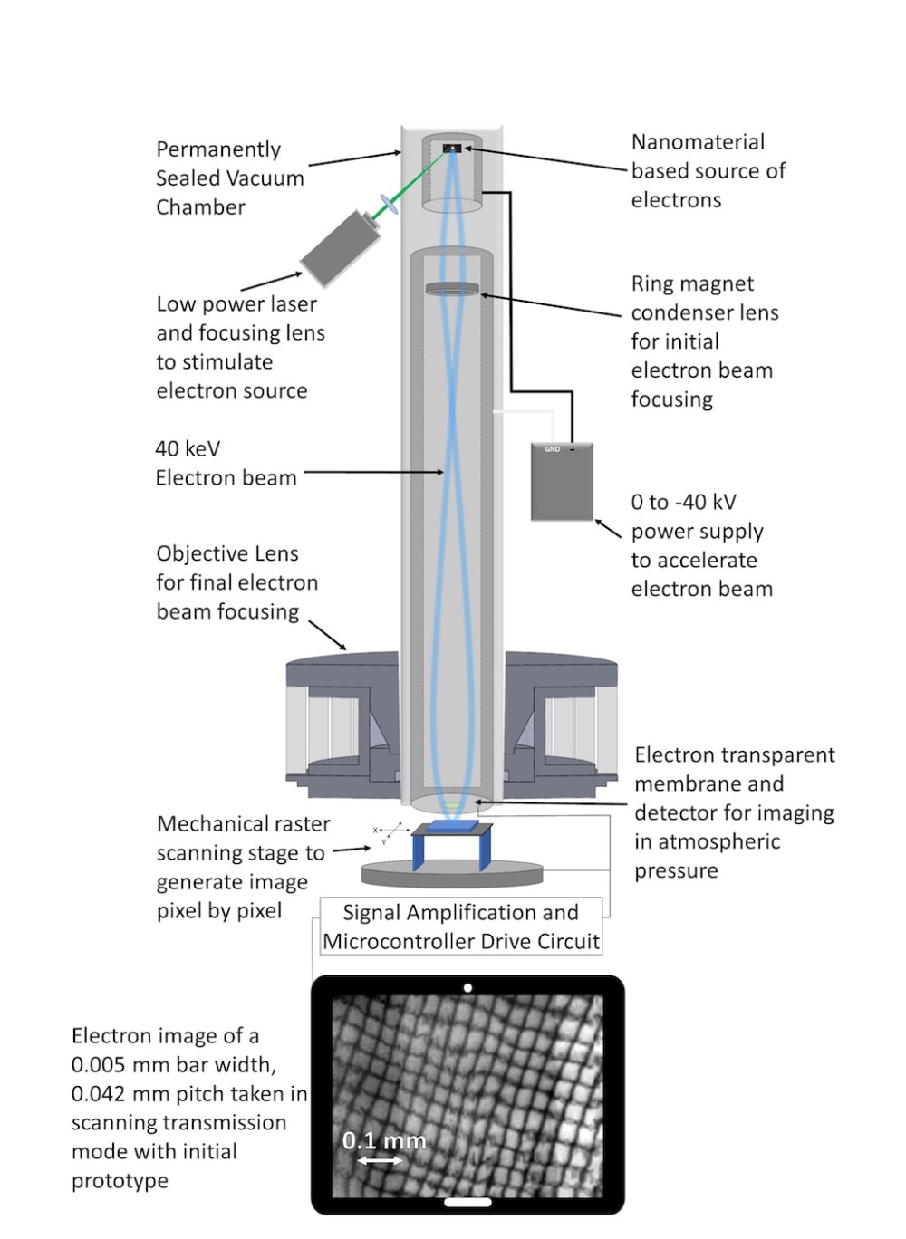
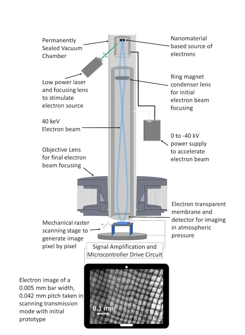
Our team at The University of British Columbia are developing a system, named AweSEM, that completely re-imagines the components of an SEM (Figure 1) to conceivably lower the cost of a single unit by 100X. This price point is in keeping with digitally integrated optical desktop microscopes. The low cost is made possible primarily through the application of a novel electron source that leverages a heat trap effect on a readily-available carbon nanomaterial. This mode of operation allows for a smaller electron emission area than compared with traditional thermionic electron sources, allowing for more simplified electron optics. The beam is contained within a permanently sealed vacuum tube that eliminates the need for active pumping (like an old cathode ray tube television) and is focused through an electron-transparent membrane using a permanent magnet lens that requires no additional power. The sample can then be imaged directly in atmosphere or a low vacuum environment, which drastically simplifies sample preparation and alleviates limitations on sample type. These factors present the opportunity for high throughput sample imaging and characterization. A mechanical stage allows sample scanning in the xy plane. A solid-state detector can be integrated with a smart device (e.g., iPhone, tablet) in order to facilitate cloud-based image processing/sharing, software enhancements, and general ease-of-use. Our proof-of-concept device can capture 1 x 1 mm images with a resolution on the order of a few microns.
The envisioned AweSEM device has the potential to transform a wide range of manufacturing environments with its ability to perform high-throughput and high-resolution imaging. Industries that would benefit from the AweSEM device include but are not limited to microfluidics, tissue engineering, and microelectronics. Constant technological advancements have realized a significant decrease in size for devices that were once on the macro scale, such as accelerometers in smartphones, or lab-on-a-chip diagnostic tools. However, the ability to visually characterize these new devices has essentially remained stagnant, with traditional SEMs utilizing many of the same principles from 50 years ago. AweSEM, with its atmospheric imaging capabilities, can be placed directly in assembly lines to enhance quality control practices with accuracy not possible in traditional optical microscopy. AweSEM will level the playing field for the creation of next generation high-tech devices with its low-cost and high-resolution capabilities.
-
Awards
-
 2019 Manufacturing/Robotics/Automation Honorable Mention
 -
 2019 Top 100 Entries
Voting
-
ABOUT THE ENTRANT
- Name:Casimir Kuzyk
- Type of entry:teamTeam members:Casimir Kuzyk
Gabriel Robinson-Leith
Alex Dimitrakopoulos
David Weekes
Fabian Pease
Alireza Nojeh - Patent status:patented