

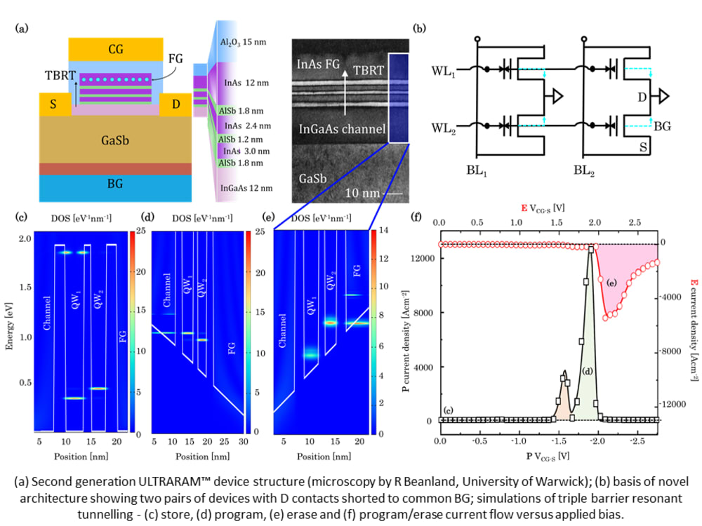


The $165bn pa memory market is dominated by DRAM ($100bn) and NAND flash ($60bn). DRAM’s high speed (compared to Flash) at low cost (compared to SRAM) has made it the main memory in all computers and electronic devices. However, it has significant drawbacks of volatility and destructive read of data. In 32 Gb DRAM chips refresh contributes to 20% of power consumption, and degrades system performance by 30% [IEEE Trans on Computers 65, 108 (2016)]. Whilst conventional emerging non-volatile (NV) memories achieved a market size of $1bn in 2019, this was limited to niche applications interfacing mass storage and DRAM. It falls short of our ambition to replace DRAM with a NV equivalent: a goal that is beyond the reach of rival NV memories due to one or more of; limited endurance, inferior speed and switching energies that are orders of magnitude higher than DRAM. We recently demonstrated room-temperature operation of patented floating-gate compound semiconductor memory cells. Exploiting the unique properties of the 6.1 A family of semiconductors (GaSb, InAs and AlSb) and resonant tunnelling, enables devices that are NV with low-voltage (≤2.6 V) write and erase, and switching energies that are 100 times lower than DRAM for the same cell size, with faster switching speeds.
Achieving manufacturability of commercially viable ULTRARAM memory chips is a huge challenge, requiring advances on three fronts: (1) fabrication of larger and larger arrays, (2) implementation on silicon wafers, and (3) scaling of feature sizes. Nevertheless, we have already developed a novel highly-compact RAM architecture (patent-pending) that facilitates record-breaking areal cell densities of 3.4F2 (F is the gate dimension), and are in the process of fabricating 2x2 bit arrays, with plans for 64 bit and 1 Mbit. We have made substantial progress implementing ULTRARAM™ on silicon, and will shortly begin scaling F from the micron to the nanometre regime. It is extremely difficult to predict the cost of ULTRARAM™ at this early stage in its development, but there are some very compelling reasons to expect the cost to be low compared to DRAM. Besides being twice as compact as DRAM (6 to 8 F2), ULTRARAM™ is expected to be simpler to manufacture and lacks DRAM’s deficiencies of refresh and non‐destructive read, eliminating the need for additional compensating circuitry, and releasing more of the chip for use by memory arrays.
While the ambitious long-term aim is to replace DRAM, we envisage ULTRARAM™ will initially be used in applications where non-volatility and ultralow energy consumption are crucial, for example autonomous Internet of Things (IoT) sensors. This will be followed by consumer devices such as smartphones and tablets where a single ULTRARAM™ chip can replace DRAM and flash, and ultimately across all IT, including laptops, PC and data centres.
M. Hayne, ‘Electronic memory devices’ US patent 10243086B2.
O. Tizno et al., ‘Room-temperature operation of low-voltage, non-volatile, compound-semiconductor memory cells’, Scientific Reports 9, 8950 (2019).
D. Lane and M. Hayne, ‘Simulations of ultralow-power nonvolatile cells for random-access memory’, IEEE Trans. Electron Devices 67, 474 (2020).
-
Awards
-
 2020 Electronics/Sensors/IoT Honorable Mention
 -
 2020 Top 100 Entries
Like this entry?
-
About the Entrant
- Name:Manus Hayne
- Type of entry:teamTeam members:Manus Hayne, Peter Hodgson, Dom Lane and Ofogh Tizno
- Software used for this entry:nextnano and SPICE
- Patent status:patented