


To increase the processing speed and reduce the power consumption of electronic devices, the microelectronics industry continues to push for increasingly smaller feature sizes. Realizing this miniaturization will require the development of robust resist materials as templates to transfer circuit patterns into device-useful substrates such as silicon.
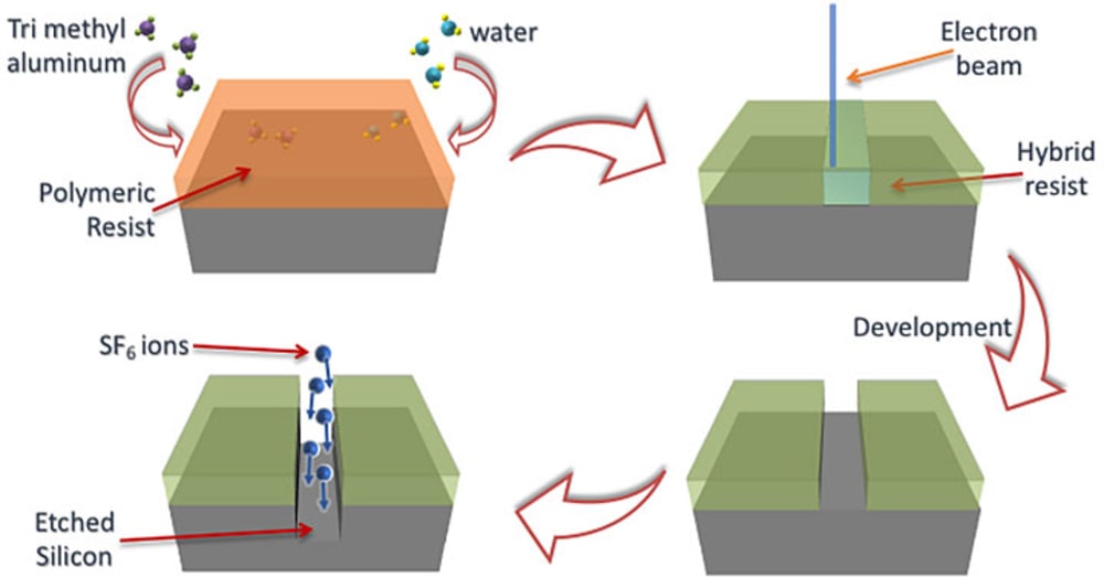
Brookhaven National Laboratory’s Center for Functional Nanomaterials (CFN) has developed a new organic-inorganic photoresist platform for such high-resolution nanopatterning of next-generation microelectronics devices. Hybrid photoresists are synthesized by infiltrating vapor-phase inorganic precursors into an organic matrix using an atomic layer deposition (ALD) system, a standard piece of nanofabrication equipment for depositing ultrathin inorganic films on surfaces. The ALD-based vapor-phase infiltration enables control over the type, molecular structure, and amount of inorganic materials that are externally incorporated into an organic thin film.
A model hybrid resist was created with inorganic aluminum oxide and organic poly(methyl methacrylate), or PMMA, the most widely used resist in electron-beam lithography, in which electrons are used to create the pattern template. This hybrid resist features 30 nm resolution, a moderate critical dose (2000 uC/cm2), and unprecedented high silicon etch selectivity (>70), enabling the patterning of 30 nm wide silicon structures with heights exceeding ~500 nm (aspect ratio ~17). These resist performance parameters can be controlled by adjusting the number of infiltration cycles. For example, after only two alumina infiltrating cycles, the silicon etch selectivity of the hybrid resist surpasses that of ZEP® (a copolymer based on methyl styrene and chloromethyl acrylate) and hydrogen silsesquioxane (HSQ), two expensive proprietary resists. After four infiltration cycles, the hybrid resist has a 40-percent-higher silicon etch selectivity than that of silicon dioxide, a hard mask layer that requires additional processing steps.
Conventional resists require complex chemical synthesis. Moreover, resist performance parameters—including critical dose, exposure contrast, and etch resistance—cannot be easily tuned per application. For example, high resolution and high contrast are needed to pattern logic devices, whereas high etch resistance is needed to pattern 3-D-stacked memory devices such as flash memories. The infiltration-based hybrid resist platform overcomes these challenges by leveraging ALD tools found in almost every nanofabrication facility and low-cost materials.
The silicon microelectronics industry is now advancing to extreme ultraviolet (EUV) lithography for the high-volume manufacture of sub-7 nm silicon transistors. However, the low EUV absorption of carbon and oxygen—both primary elements in typical organic-based EUV photoresists—causes low EUV sensitivity. These resists can be chemically modified to amplify their response to EUV light, but such chemical amplification leads to patterning blur unsuitable for fabricating sub-7 nm silicon structures. With the infiltration-based hybrid resist platform, inorganic elements with high EUV absorption (e.g., tin and hafnium) can be controllably incorporated without complex chemical synthesis. Thus, the platform is a promising technology for the fabrication of high-sensitivity, high-resolution, and high-etch-resistance EUV resists.
As separately demonstrated at the CFN, the platform can also be used to synthesize other hybrid coatings with chemical sensing capabilities or ultrahigh capacities for mechanical energy storage.
-
Awards
-
 2020 Top 100 Entries
Like this entry?
-
About the Entrant
- Name:Ariana Manglaviti
- Type of entry:teamTeam members:Chang-Yong Nam, Staff Scientist, Center for Functional Nanomaterials, Brookhaven National Laboratory; Adjunct Professor, Department of Materials Science and Chemical Engineering, Stony Brook University
Ming Lu, Staff Scientist, Center for Functional Nanomaterials, Brookhaven National Laboratory
Aaron Stein, Staff Scientist, Center for Functional Nanomaterials, Brookhaven National Laboratory
Kim Kisslinger, Advanced Technical Associate, Center for Functional Nanomaterials, Brookhaven National Laboratory
Nikhil Tiwale, Research Associate, Center for Functional Nanomaterials, Brookhaven National Laboratory
Jiyoung Kim, Professor, Department of Electrical and Computer Engineering, University of Texas at Dallas
Ashwanth Subramanian, Graduate Research Assistant, Center for Functional Nanomaterials, Brookhaven National Laboratory; PhD Student, Department of Materials Science and Chemical Engineering, Stony Brook University - Patent status:pending