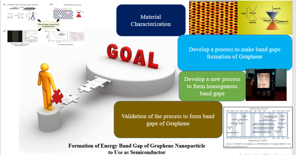

The thinnest material in existence is Graphene. It has high thermal conductivity, quantum hall effect, mechanical good with high Young's modulus (1 TPa) and intrinsic strength of 130 GPa, high optical transmittance and high electronic transport, barrier and flame retardant properties owing to their zero bad gaps as a single sheet. Graphene is a 2D structure of carbon atoms with hexagonal crystalline structure with sp2 bonds. Graphene, being a gapless semiconductor, cannot be used in pristine form for nano-electronic applications. Therefore, it is essential to generate a finite gap in the energy. Its recent experimental discovery has stimulated extensive investigations on every aspect of this novel material. The recent work indicates that the carbon layer is covalently bonded to the SiC sub-lattice. However, due to the weak lattice deformation induced by uniaxial or in-plane shear strain, most strained graphene studies have yielded bandgaps <1 eV. In this work, a modulated inhomogeneous local asymmetric elastic–plastic straining is reported that utilizes GPa-level laser shocking at a high strain rate (dε/dt) ≈ 106–107 s−1, with excellent formability, inducing tunable bandgaps in graphene of up to 2.1 eV, as determined by scanning tunneling spectroscopy. High-resolution imaging and Raman spectroscopy reveal strain-induced modifications to the atomic and electronic structure in graphene and first-principles simulations predict the measured bandgap openings. Laser shock modulation of semi-metallic graphene to a semiconducting material with controllable bandgap has the potential to benefit the electronic and optoelectronic industries. Moreover, modulation of the Fermi level of graphene over a large range is also very difficult to circumvent heterojunction energy barriers, thus further limiting the development of graphene-based electronic or optoelectronic devices.
Although extrinsic approaches to open the bandgap and modulate the work function of graphene have been attempted, including doping hydrogen adsorption formation of graphene nanostructures and multilayers, they have not yet been able to tune work function and yielded large bandgaps (always <1 eV); [27] as a result, the device performance based on graphene is still under restriction. Hence, an alternative method to modulate the electron energy structure of graphene is required to fully realize the potential of graphene in future semiconductor industry. The research gap is that as the 2D graphene is highly conductive, it should be transformed in to semi conductive material. In addition to that as the existing process of transforming graphene as semi conductive is nonhomogeneous. This approaches can be applied to make it homogeneous.
Electrospining set-up consisted of a high voltage supply (-20 KV and +50KV), a syringe pump (TL-F6, Tong Li Tech, China), a drum collector (Diameter-158mm, Length-500mm, 500 rpm), a syringe, a heater (0.5 KW) and needles (20g). All the components were used as a single electrospinning machine (Model: TL-Pro-BM, Company: Tong Li Tech, Origin: China). At first syringe was filled up with required amount of solution and then placed into the pump and connected to needles by a pipe. Aluminum foil was wrapped on the surface of drum collector and negative voltage connection was connected to collector.
Like this entry?
-
About the Entrant
- Name:Prof. Dr. Mohammad Asaduzzaman Chowdhury
- Type of entry:teamTeam members:Prof. Dr. Mohammad Asaduzzaman Chowdhury, Rajib Nandee, Bengir Ahmed Shuvho
- Software used for this entry:YASARA and COMSOL
- Patent status:none